Facebook
 Google
 GitHub
 Linkedin
C
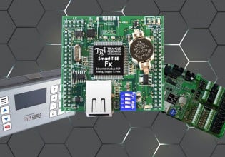
Hi all Someone asked what to do with the materials to make the board. I thought I'd at least provide the outline of how to do it. 1 get the tgz 2 make a directory on your Linux box, put the .tgz there and do tar -czvf dio.tgz 3 you now have a directoty with various files. 4 what you do from here varies with the board fab house. I'll use Alberta Printed Circuits since that is who I used. 5 there are quite a few DIO484.output_*.gbx files. These are the gerber files for the various layers. solder side, component side, silkscreens, yada yada. You may need all of them for production boards. I used the solder and component side layers and a NC drill file. There is complete documentation on the APCircuits website on what to do with PCB's output to get it in shape for their process. I used their proto 1 service which is simple two sided pth (plated through holes) boards with no soldermask or silkscreen, etc. Two day turn. If you want to use APCircuits I can give you the files, properly named that I used. 6 if you are going to deal with a different fab, I would get pcb (www.rpmfind.com) and load the DIO484 file. This is the actual board layout. You can then print postscript versions of the layers that will help you equate them to what the fab house wants. These are handy enough that the next tarball I send will include them 7 (A miracle happens) You now have blank boards. There is a bill of materials that lists all the components you need to build the boards, quantities and who I got them from so you can get an idea about pricing, etc. 8 get the stuff and solder it on the board. The board is made for hand assembly, but there is a lot of soldering and some chance for bridges and shorts. You are looking at the component side when you have the ribbon cable connector to your left and the LinuxPLC Project line below it is rtght side up. All chips have pin 1 to the left and marked with a square pad, The three 18 pin chips at the top are the drivers. The spots for a component to the right of each is for the 1uF mono ceramic cap. The next row are optoisolators (6) and the row of components below that are 2.2k resistors The next row of chips are the optoisolators for the inputs and below that are the input voltage dividers. They go from left to right 3.3k, 680, 3.3k 680, etc. the row of pads between the resistors and the optos are for small .1uF capacitors for filtering if needed.. 9 I would mount the discrete components first, then the IC's then the connectors. I'll be happy to answer questions or suggestions to make this clearer. Regards cww _______________________________________________ LinuxPLC mailing list [email protected] http://linuxplc.org/mailman/listinfo/linuxplc