 Facebook
 Google
 GitHub
 Linkedin
Analog Signal Conditioning and Referencing
Modern analog-to-digital converters are phenomenally accurate, dependable, repeatable, and surprisingly inexpensive as integrated circuits considering their capabilities. However, even the best ADC is useless in a real application unless the analog voltage signal input to it is properly conditioned, or “made ready” for the ADC to receive. We have already explored one form of signal conditioning for ADC circuits, and that is the anti-alias filter, designed to block any signals from reaching the ADC with frequencies higher than the ADC can faithfully sample. An even more fundamental signal-conditioning requirement, though, is to ensure the analog input signal voltage is a good match for the voltage range of the ADC.
Most analog signals take the form of a varying voltage, but not all voltages are equally referenced. Recall the fundamental principle in electricity that “voltage” or “potential” is a quantity: there is no such thing as a voltage existing at a single point. Voltage is something that exists between two points. In electronic circuits, most voltage signals are referenced to a common point called “ground.” However, in many industrial measurement applications, the voltage signal of interest may not have one of its poles connected to ground. A voltage source may be “floating,” as in the case of an ungrounded thermocouple junction. A voltage source may also be “elevated,” which means both of its connection points are at some substantial amount of voltage with reference to ground. Whether or not a voltage signal source is “referenced” to ground poses a challenge for accurate and safe signal measurement, and it is a subject fraught with much confusion. This section of the book will explore some of these principles and applications, showing how to properly connect data acquisition (DAQ) hardware to voltage signal sources so as to overcome these problems.
Instrumentation amplifiers
To illustrate the necessity of signal conditioning, and to introduce a critically important conditioning circuit called an “instrumentation amplifier,” let us examine a data acquisition application applied to a photovoltaic power system (solar electric panel) generating electricity from sunshine. Here, our goal is to use a pair of analog-to-digital converter circuits to monitor the solar panel’s voltage as well as its output current to the DC load. Since ADC circuits typically require voltage signals rather than current, a precision shunt resistor is placed in series with the solar panel to produce a measurable voltage drop directly proportional to load current:
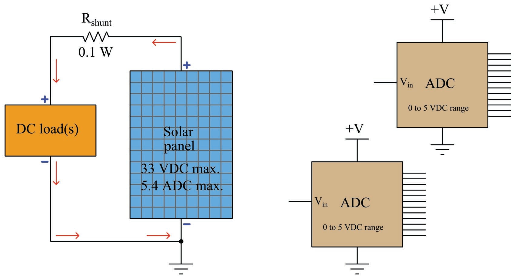
The question we face now is, “how do we connect each ADC to the photovoltaic power system?” Each ADC is designed to digitize a DC voltage signal with reference to its ground connection, 0 to 5 volts DC producing a full range of “count” values. Right away we see that the maximum output voltage of the photovoltaic panel (33 volts DC) significantly exceeds the maximum input range of each ADC (5 volts DC), while the voltage produced by the shunt resistor for measuring load current will be very small (0.54 volts DC) compared to the input range of each ADC. Excessive signal voltage is obviously a problem, while a small voltage range will not effectively utilize the available measurement span or signal resolution.
The first problem – how to measure panel voltage when it greatly exceeds the ADC’s 5-volt maximum – may be easily solved by connecting one ADC to the panel through a precision voltage divider. In this particular case, a 10:1 divider circuit will do nicely:

With this 10:1 voltage divider circuit in place, the panel’s 33 VDC maximum output will be seen as a 3.3 VDC maximum signal value at the ADC, which is both within its measurement range and yet spans a majority of the available range for good measurement resolution. This simple voltage divider network thus conditions the solar panel’s 33 volt (maximum) output to a range acceptable to the ADC. Without such a divider in place, the ADC would be over-ranged at the very least – but most likely destroyed – by the solar panel’s relatively high voltage.
Please note how the ADC is really nothing but a voltmeter: sampling whatever voltage it senses between its \(V_{in}\) terminal and its Ground terminal. If you wish, you may visualize the ADC as being a voltmeter with red and black test leads, the red test lead being \(V_{in}\) and the black test lead being Ground.
Connecting the second ADC to the shunt resistor presents an even greater challenge, as we see in the following schematic. Treating the second ADC as a voltmeter (its “red” test lead being the \(V_{in}\) terminal and its “black” test lead being the Ground terminal), it might seem appropriate to connect those two terminals directly across the shunt resistor. However, doing so will immediately result in the panel’s full current output flowing through the Ground conductors:
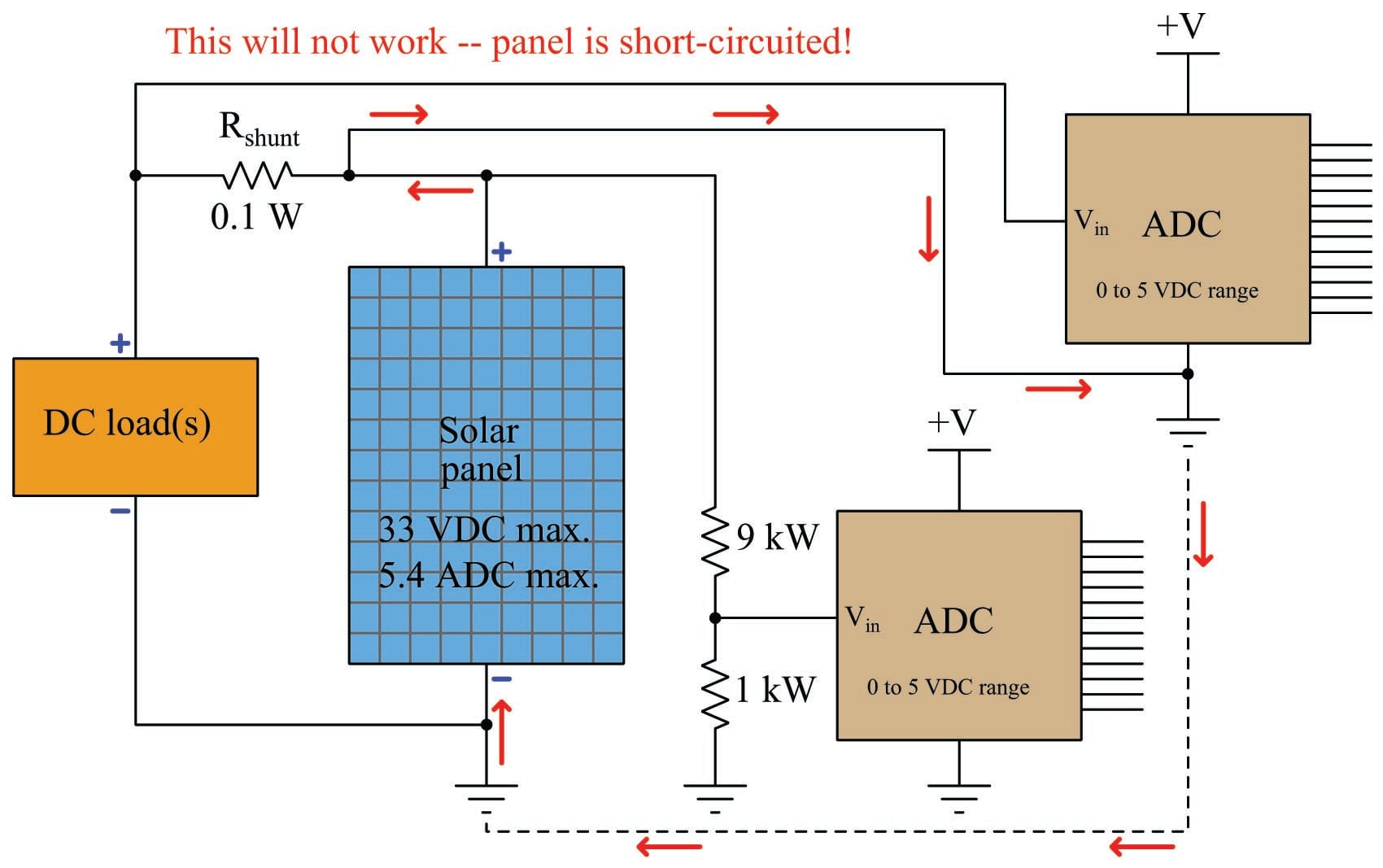
Attempting to connect the ADC in parallel with the shunt resistor in order to measure its voltage drop results in unintentionally short-circuiting the solar panel through the ADC’s ground connection, as shown by the “fault current” path depicted in the schematic! Not only will this circuit configuration fail to function properly, but it may even result in overheated conductors. A failure to recognize the measurement problems inherent to “elevated” voltage signals is no academic matter: a mistake like this could very well end in disaster, especially if the power source in question is much larger than a single solar panel!
One way to try eliminating the fault current path is to avoid connecting the ADC to the same signal ground point shared by the first ADC. We could power the second ADC using a battery, and simply let it “float” at an elevated potential (up to 33 volts) from ground:
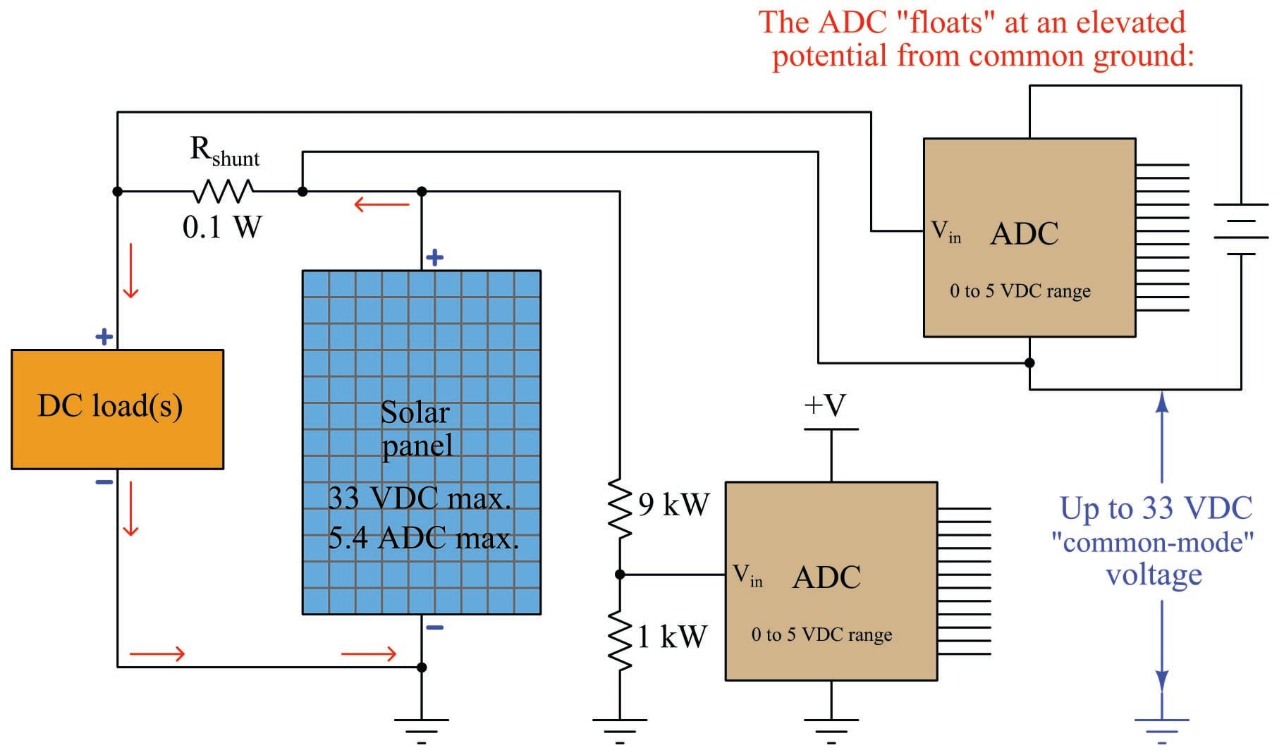
While this “floating ADC” solution does avoid short-circuiting the solar panel, it does not completely eliminate the fundamental problem. When we connect the ADCs’ digital output lines to a microprocessor so as to actually do something useful with the digitized signals, we face the problem of having the first ADC’s digital lines referenced to ground, while the second ADC’s digital lines are at an elevated potential from ground (up to 33 volts!). To a microprocessor expecting 5.0 volt TTL logic signals (0 volts = “low”, 5 volts = “high”) from each ADC, this makes the second ADC’s digital output unreadable (33 volts = ???, 38 volts = ???). The microprocessor must share the same ground connection as each ADC, or else the ADCs’ digital output will not be readable.
We refer to the added 33 volts as a common-mode voltage because that amount of voltage is common to both poles of the signal source (the shunt resistor terminals), and now is common to the digital output lines of the ADC as well. Most sensitive electronic circuits – microprocessors included – cannot effectively interpret signals having significant common-mode voltages. Somehow, we must find a way to eliminate this common-mode potential so that a microprocessor may sample both ADCs’ digital outputs.
An elegant solution to this problem involves the use of a differential amplifier to sample the voltage drop of the shunt resistor, then translate that voltage drop into a ground-referenced voltage ready for input to the second ADC, sharing the same ground as the first ADC. So long as this differential amplifier can tolerate the 33 VDC “common mode” voltage presented by the shunt resistor’s location on the ungrounded side of the solar panel, the shunt resistor’s signal will be properly conditioned for the ADC:
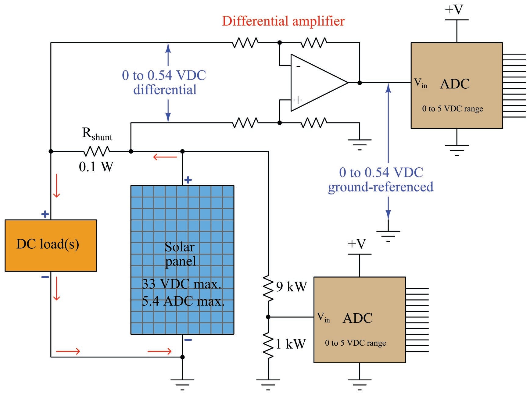
The task of the differential amplifier is to take the difference in potential between its two input lines and repeat that voltage at its output terminal, with reference to ground: effectively “shifting” the common-mode voltage from 33 volts to 0 volts. Thus, the differential amplifier takes a “floating” voltage signal and converts it into a ground-referenced voltage signal.
The following schematic shows how the differential amplifier does this, assuming a condition of maximum solar panel voltage and current (33 volts at 5.4 amps), and equal-value resistors in the differential amplifier circuit:
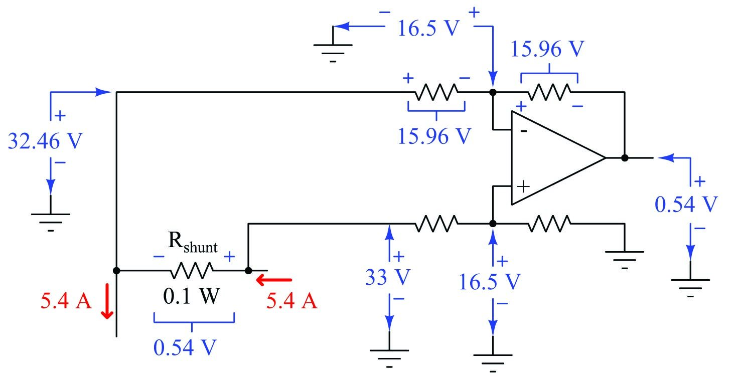
All voltages in the above schematic may be derived from the signal source (shunt resistor) and the general rule that an operational amplifier does its best to maintain zero differential voltage between its input terminals, through the action of negative feedback. The lower voltage-divider network presents half of the 33 volt solar panel potential (with reference to ground) to the noninverting opamp terminal. The opamp does its best to match this potential at its inverting input terminal (i.e. trying to keep the voltage difference between those two inputs at zero). This in turn drops 15.96 volts across the upper-left resistor (the difference between the “downstream” shunt resistor terminal voltage of 32.46 volts and the 16.5 volts matched by the opamp, both with respect to ground). That 15.96 volt drop results in a current through both upper resistors, dropping the same amount of voltage across the upper-right resistor, resulting in an opamp output voltage that is equal to 0.54 volts with respect to ground: the same potential that exists across the shunt resistor terminals, just lacking the common-mode voltage.
Not only does a differential amplifier translate an “elevated” voltage signal into a ground-referenced signal the ADC can digitize, but it also has the ability to overcome another problem we haven’t even discussed yet: amplifying the rather weak 0 to 0.54 volt shunt resistor potential into something larger to better match the ADC’s 0 to 5 volt input range. Most of the ADC’s 0 to 5 volt input range would be wasted digitizing a signal that never exceeds 0.54 volts, so amplification of this signal by some fixed gain would improve the resolution of this data channel.
Fortunately, it is a rather simple matter to equip our differential amplifier circuit with variable gain capability by adding two more operational amplifiers and three more resistors. The resulting configuration is called an instrumentation amplifier, so named because of its versatility in a wide variety of measurement and data acquisition applications:
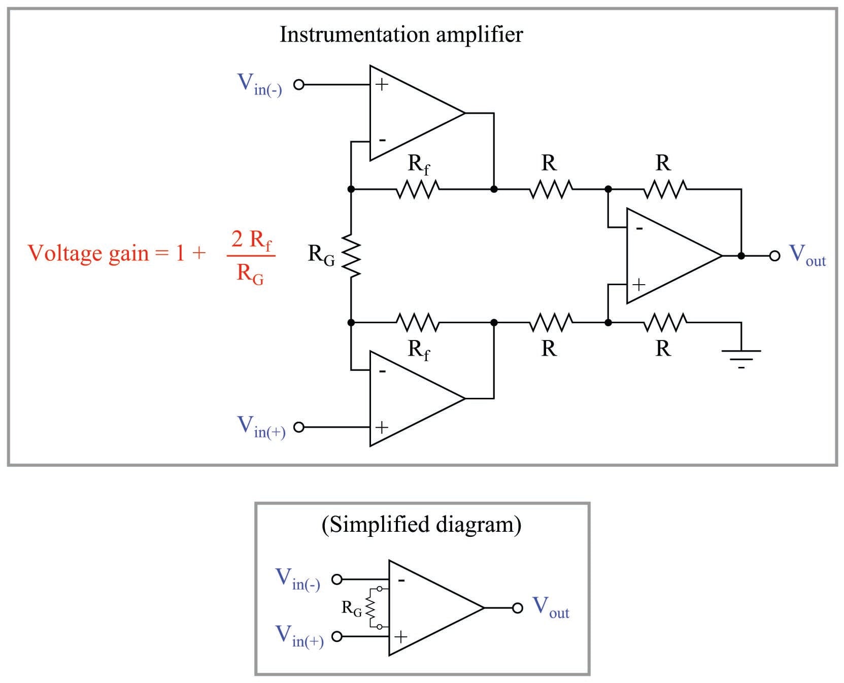
A very convenient feature of the instrumentation amplifier is that its gain may be set by changing the value of a single resistor, \(R_G\). All other resistors in an instrumentation amplifier IC are laser-trimmed components on the same semiconductor substrate as the opamps, giving them extremely high accuracy and temperature stability. \(R_G\) is typically an external resistor connected to the instrumentation amplifier IC chip by a pair of terminals.
As the formula shows us, the basic gain of an instrumentation amplifier may be adjusted from 1 (\(R_G\) open) to infinite (\(R_G\) shorted), inclusive. The input voltage range is limited only by the opamp power supplies. Thus, the instrumentation amplifier is a versatile signal-conditioning circuit for translating virtually any voltage signal into a ground-referenced, buffered, and amplified signal suitable for an analog-to-digital converter.
A typical DAQ (Data AcQuisition) module will have one instrumentation amplifier for every analog-to-digital converter circuit, allowing independent signal conditioning for each measurement “channel”:
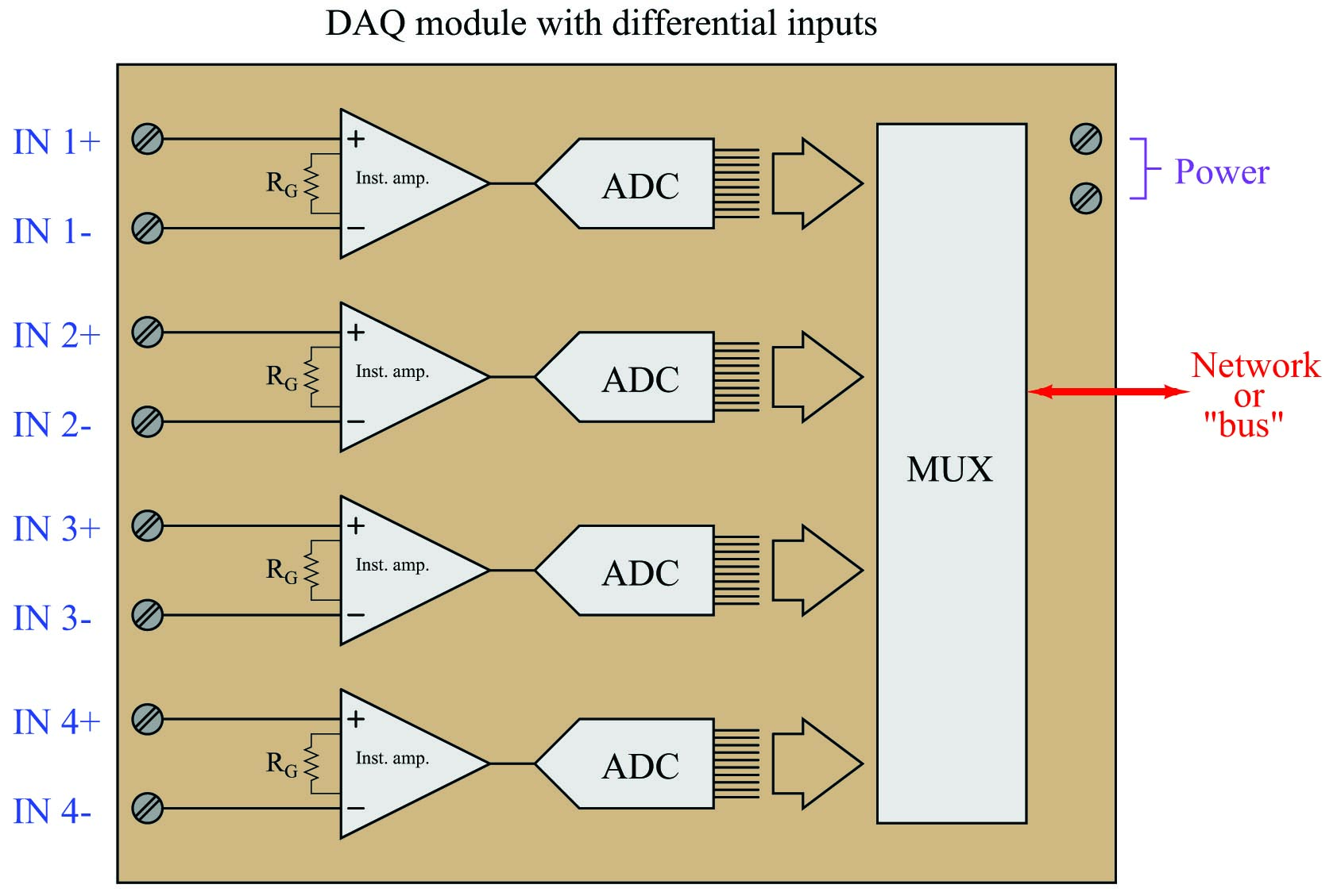
The “MUX” module shown inside this data acquisition unit is a digital multiplexer, sequentially sampling the count values output by each ADC (one at a time) and transmitting those digital count values out to the network or “bus” cable to be read by some other digital device(s).
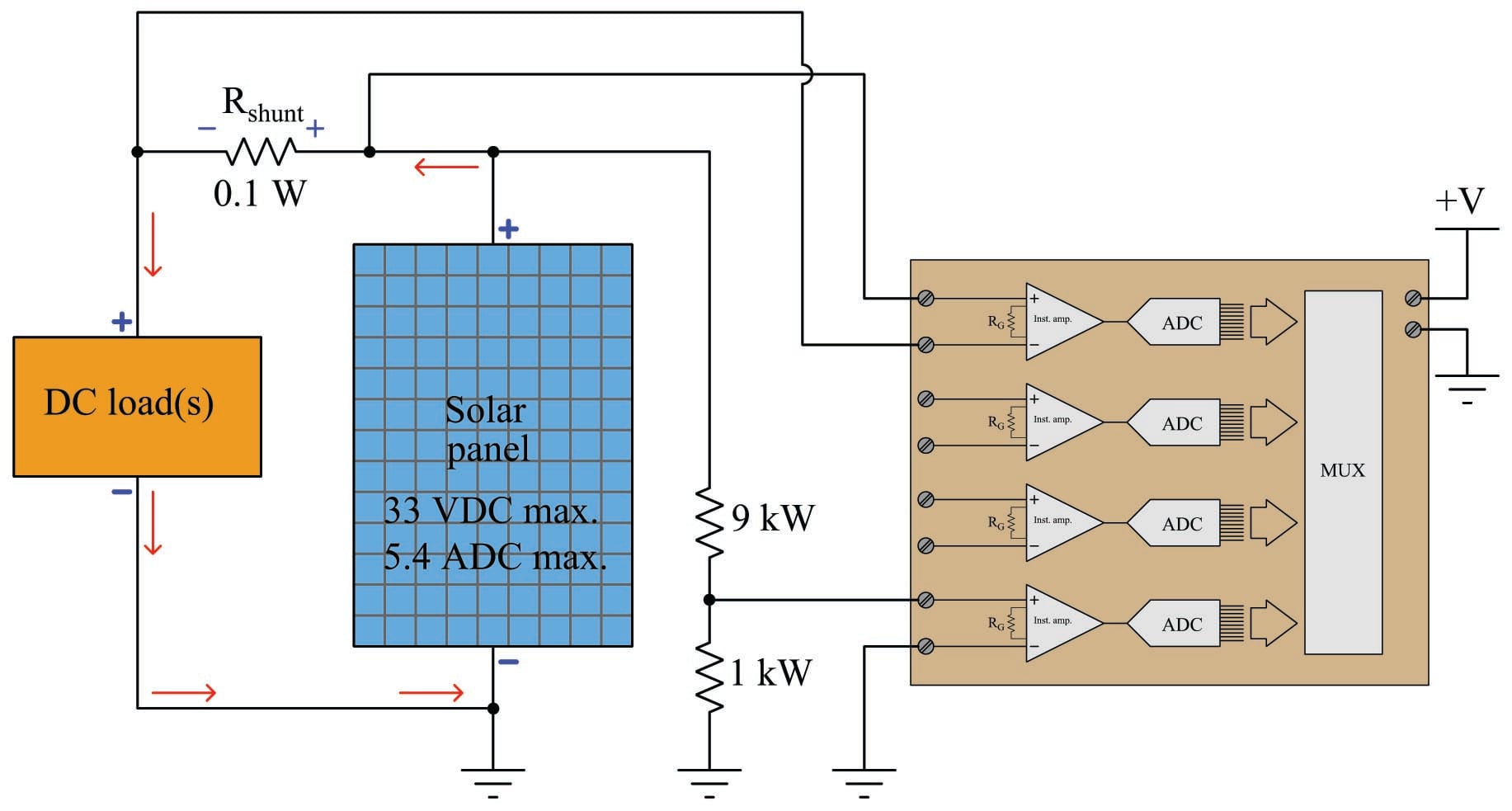
A final solution showing this DAQ module measuring solar panel voltage as well as current appears here:
Analog input references and connections
Most analog signals in industry come in the form of voltages. Even the ubiquitous 4 to 20 milliamp DC analog signal standard is typically converted into a 1 to 5 volt DC voltage signal before entering an electronic recorder, indicator, or controller. Therefore, the most common form of data acquisition device for analog measurement is one that accepts a DC voltage input signal. However, voltage signals cannot all be treated the same, especially with regard to a very important concept called ground reference. This portion of the book is devoted to an exploration of that concept, and how we may measure different kinds of voltage signals with real data acquisition devices.
First, let’s examine some examples of analog voltage signal sources. For consistency, we will focus on different circuits that all sense temperature and output proportional DC voltages. Our first example is a simple voltage-divider circuit using an RTD (Resistance Temperature Detector) as the primary sensing element. An RTD is a variable resistance with a positive temperature coefficient: increasing resistance as temperature increases. Connected as shown, it will generate a signal voltage roughly proportional to sensed temperature:
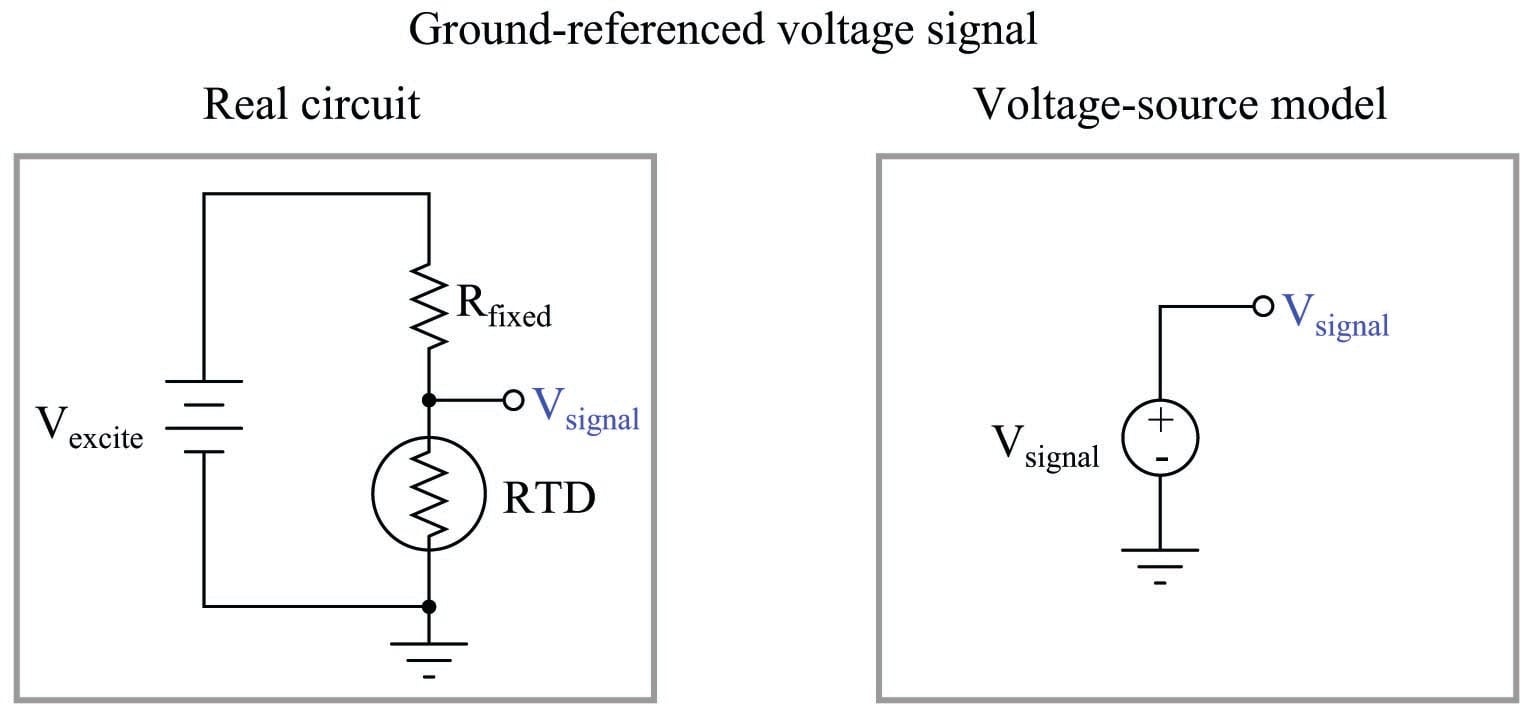
The power source for this circuit is commonly referred to as an “excitation” source, hence the label \(V_{excite}\). The voltage signal measurable across the RTD is what we might refer to as a ground-referenced voltage signal, because one pole of it is directly connected (common) to ground.
Our next example is a device called a thermocouple – a pair of dissimilar-metal wires joined together to form a junction. Thermocouple junctions produce small amounts of voltage directly proportional to temperature. As such, they are self-powered devices, needing no “excitation” power sources to operate:
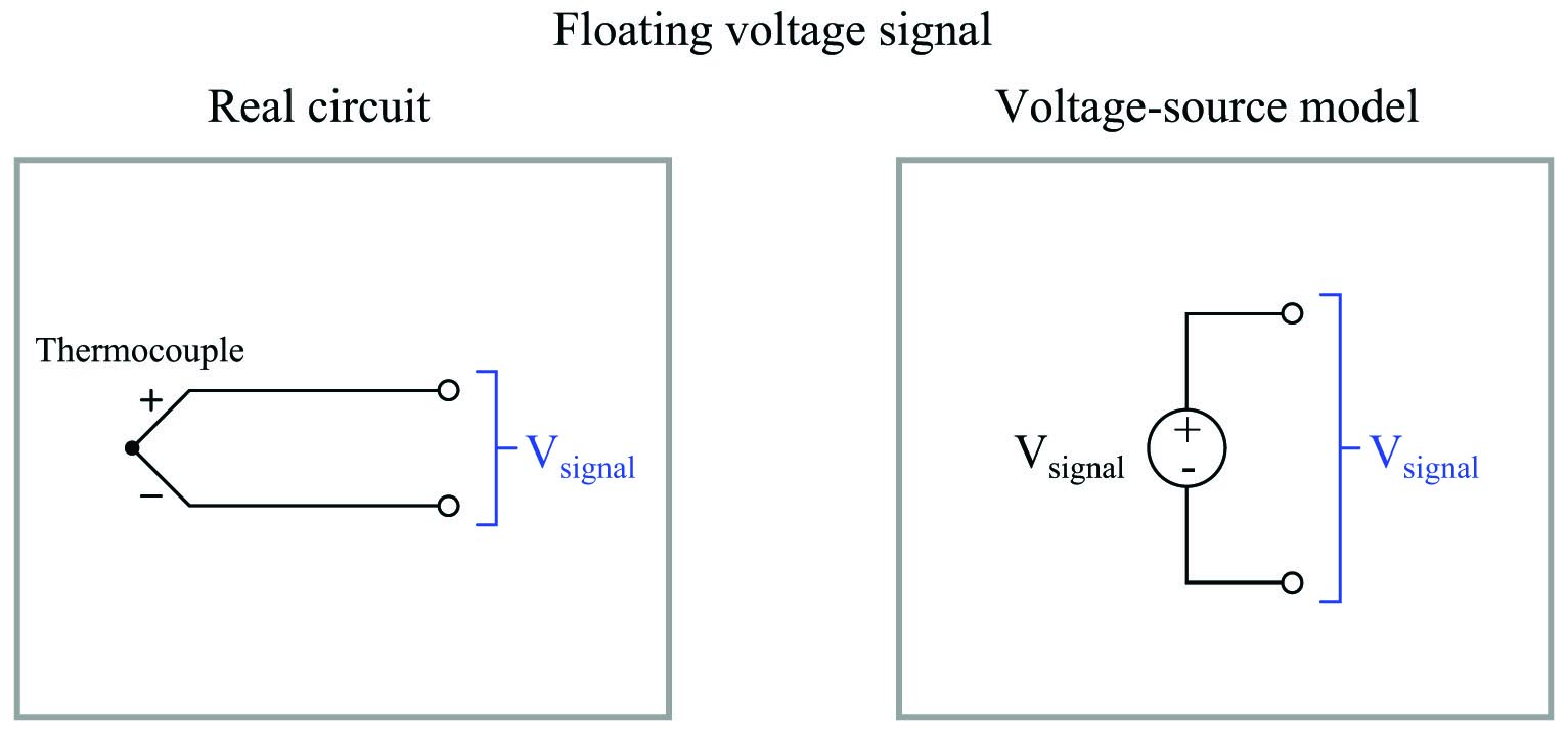
If the thermocouple junction is insulated from earth ground, we refer to it as a floating voltage signal. The word “floating” in this context refers to a complete lack of electrical connection to earth ground.
Returning to the use of RTDs for measuring temperature, another circuit design is the so-called bridge configuration, where an RTD comprises one or more “active” legs of a dual voltage divider. The excitation voltage source connects across two opposite ends of the bridge (powering both voltage dividers), while the signal voltage is measured across the other two opposite ends of the bridge (from one divider mid-point to the other):
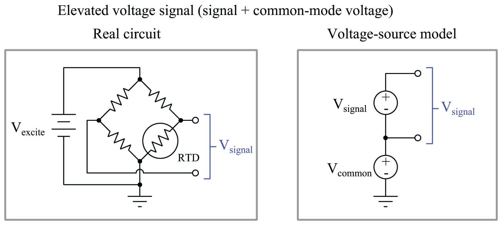
The purpose of a bridge circuit is to subtract the “live zero” voltage otherwise dropped by the RTD, which cannot produce a zero-ohm resistance at any temperature. This makes it possible to have a signal voltage range beginning at 0 volts, even though the RTD’s resistance will always be non-zero. The price we pay for this elimination of signal offset is the elevation of the signal from ground potential.
If the fixed-value resistors on the left-hand side of this bridge circuit each have the same resistance, the “common-mode” voltage will be one-half the excitation voltage. This presents an interesting situation from the perspective of measuring \(V_{signal}\), as the common-mode voltage may greatly exceed the signal voltage. We are not particularly interested in measuring the common-mode voltage because it tells us nothing about the sensed temperature, yet this relatively large voltage is “elevating” our signal voltage from ground potential whether we like it or not, and any data acquisition hardware we connect to the bridge circuit must deal effectively with this common-mode voltage (i.e. not let it corrupt or otherwise influence the accuracy of the desired signal measurement).
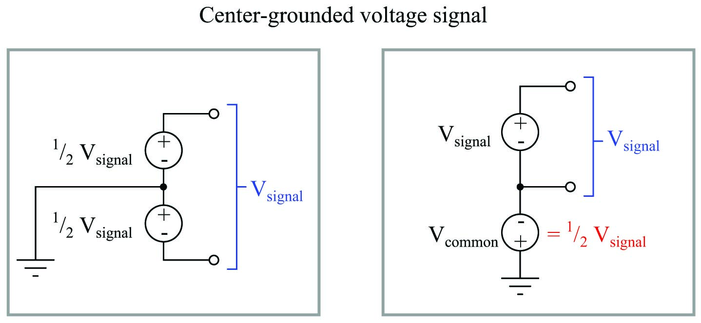
Yet another type of analog voltage signal is one where the signal is “centered” around ground potential, as is the case with a grounded-tip thermocouple:
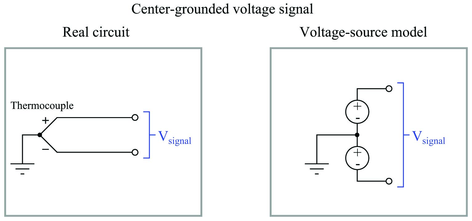
If the centering is perfectly symmetrical, the signal voltage will be evenly “split” about ground potential. The two poles of a 30 millivolt thermocouple signal, for example, will measure +15 mV and \(-15\) mV from ground. This is electrically equivalent to the elevated voltage signal model except with a negative common-mode voltage equal to half the signal voltage:
The type of analog voltage signal posed by our measurement application with becomes relevant when we connect it to a data acquisition device. Floating, ground-referenced, and elevated voltage signal sources each pose their own unique challenges to measurement, and any engineer or technician tasked with accurately measuring these signal types must understand these challenges. Data acquisition devices come in more than one type as well, and must be matched to the type of voltage signal in order to achieve good results.
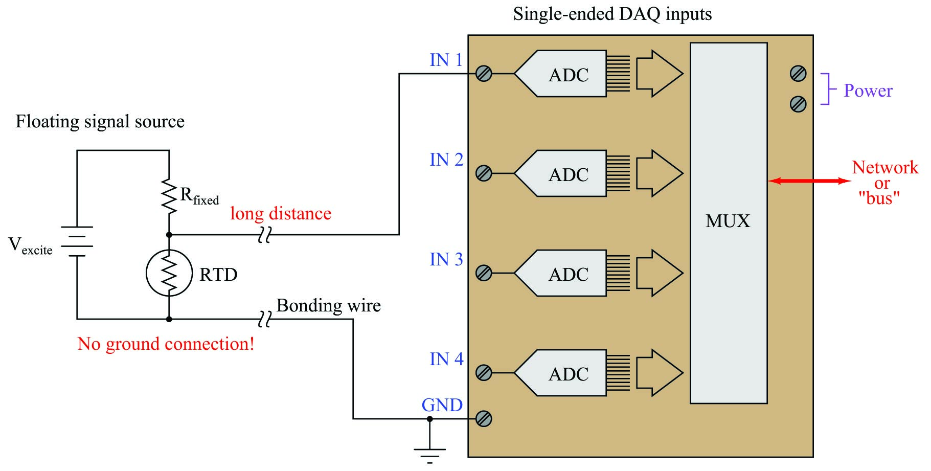
Let’s begin with our ground-referenced signal source: the simple RTD/resistor voltage divider circuit. If the divider is located close to the data acquisition (DAQ) analog input device, a single wire will suffice for connecting the two:
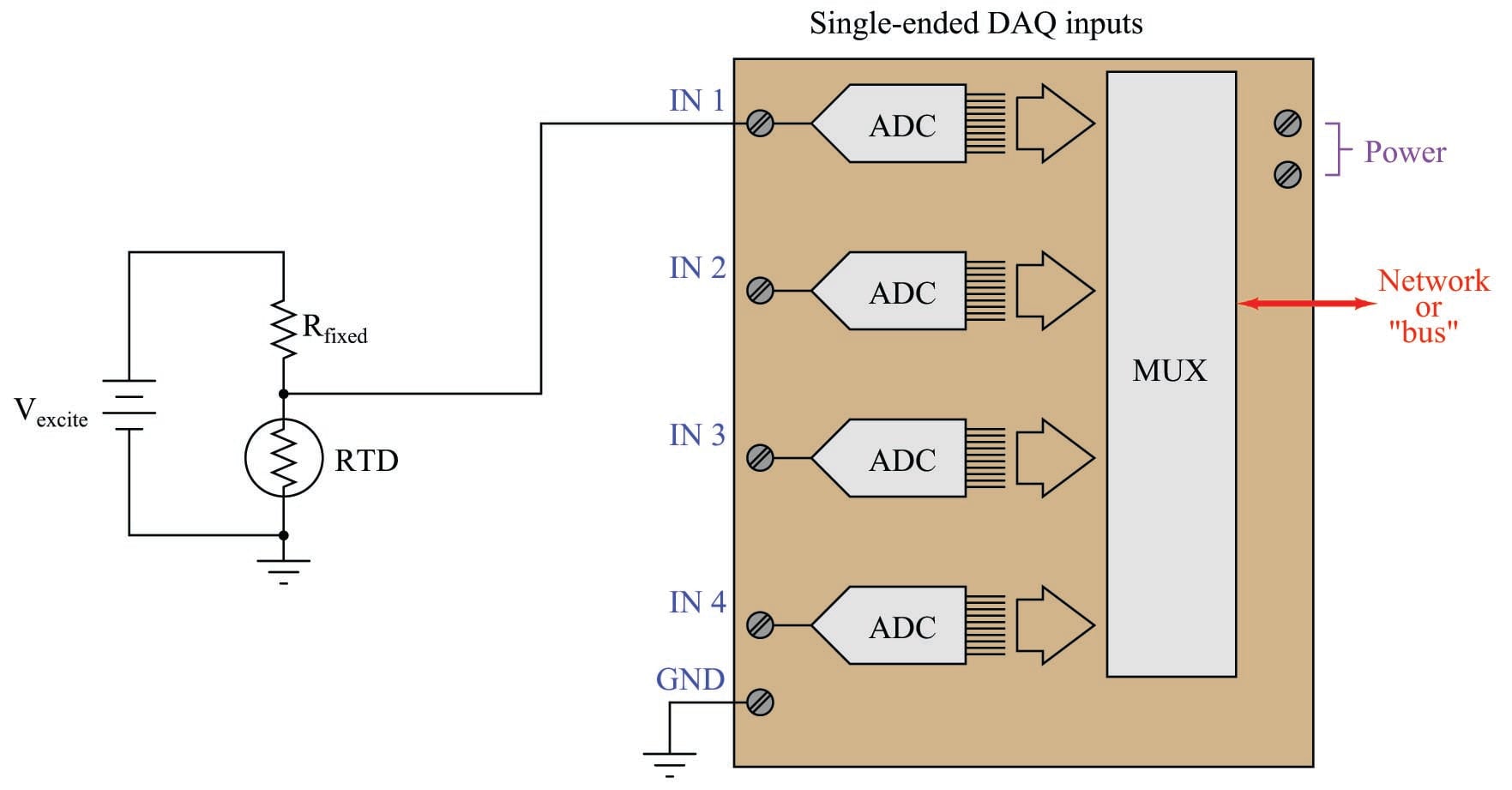
Each analog-to-digital converter (ADC) inside the DAQ unit is built to digitize a voltage with reference to ground, which is exactly the type of signal generated by our simple RTD voltage divider circuit. This type of DAQ analog input is called single-ended, and it is generally the default configuration on inexpensive DAQ units.
We cannot simply connect a single-ended DAQ input to a ground-referenced signal source using a single wire, however, if the two are located far apart from each other:
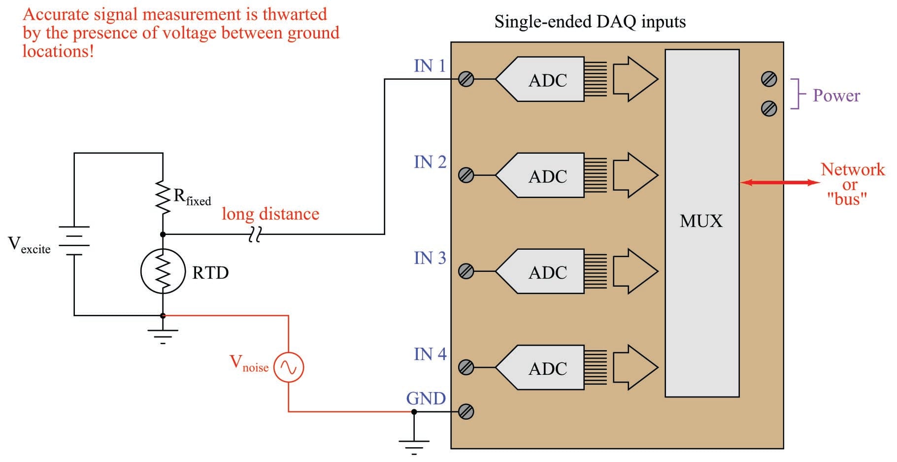
The problem here is that “all grounds are not created equal” over significant distances. If the ground path is literally through the earth (soil), there will be a myriad of noise sources adding spurious voltage to the measured signal: lightning strikes, ground leakage currents from AC power devices, and other sources of “noise” potential will become a part of the signal loop. Even continuous-metal ground paths over long distances can incur voltage drops significant enough to corrupt precision signal measurements. The grounding conductors used in AC power systems, for example, while continuous (no interruptions) between all points of use in the power system still drop enough millivoltage to significantly compromise instrumentation signals.
In essence, what appears to be a ground-referenced voltage signal source is actually an elevated voltage signal source, with the common-mode voltage being “noise” present between the two different ground locations.
At first, it would seem that connecting the two grounds together with a dedicated length of wire would solve the differential ground problem. Unfortunately, it does not. The noise sources intercepted through the earth are often of significant power, which just means any conductor stretched between two different earth grounds may end up carrying substantial amounts of current, and subsequently dropping voltage along the way due to wire resistance (\(V_{noise} = I_{ground} R_{wire}\)).
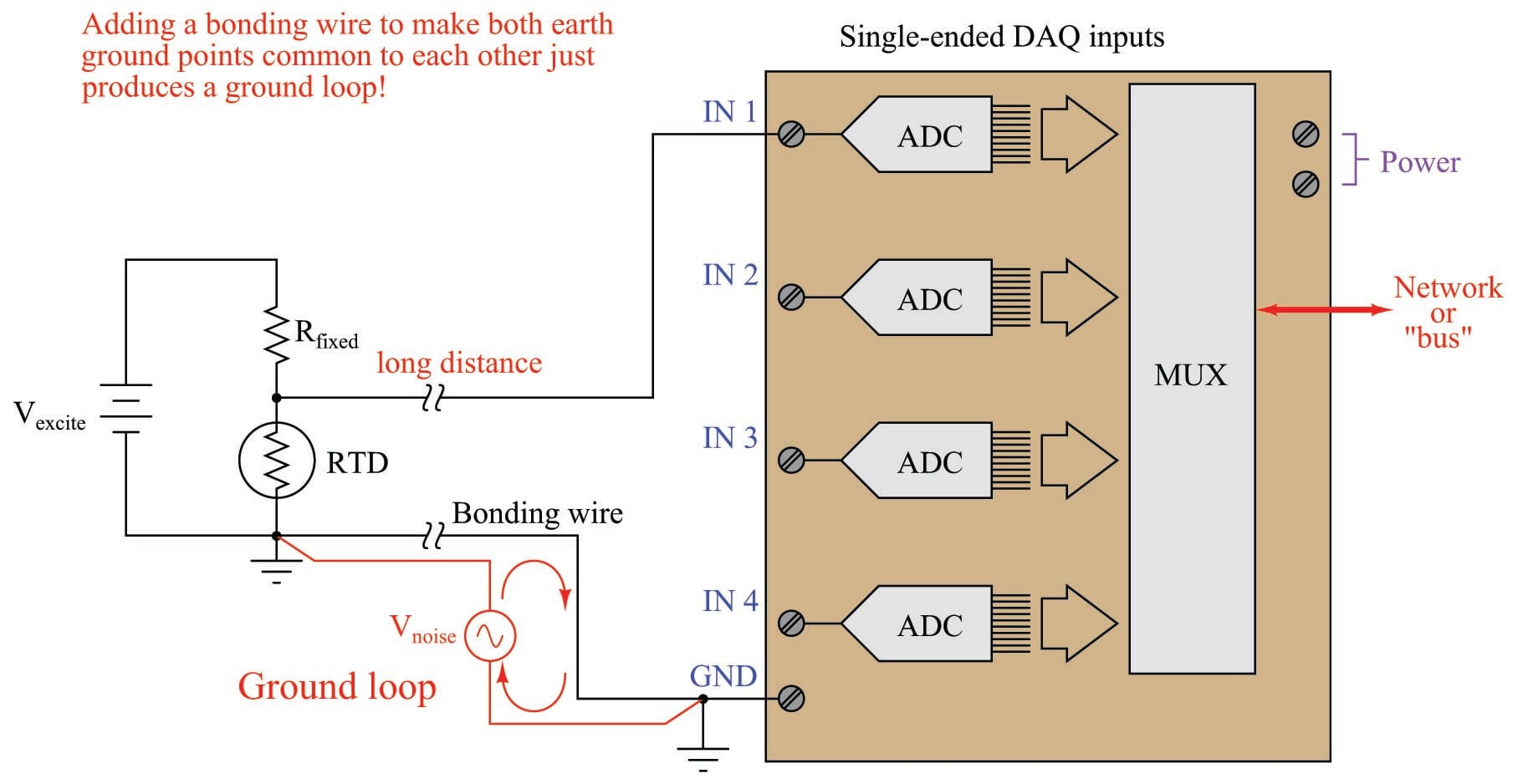
This is called a ground loop, and it should be avoided in signal circuits at all cost! Not only may the ground currents still produce significant noise voltage in the measurement circuit, but the ground currents may even become strong enough to damage the bonding wire! Ground loops are often unintentionally formed when the shield conductor of a long signal cable is earth-grounded at both ends.
A reasonable question to ask at this point is, “What constitutes a long distance when connecting ground-referenced signal sources to DAQ modules?” A simple rule to follow is that one cannot rely on ground points to be electrically common to each other (at least not common enough for precise signal-measurement purposes) if those points lie outside the same metal enclosure. If the signal source and DAQ analog input physically dwell inside the same metal enclosure, you can probably rely on the ground points being truly common to each other. If not, you should use some other means of measuring the signal. When in doubt, a sure test is to actually measure the potential difference between the source and DAQ ground points to see if any exists, being sure to check for AC noise voltage as well as DC.
Here is an example of a single-ended DAQ module successfully measuring a voltage signal source located far away:
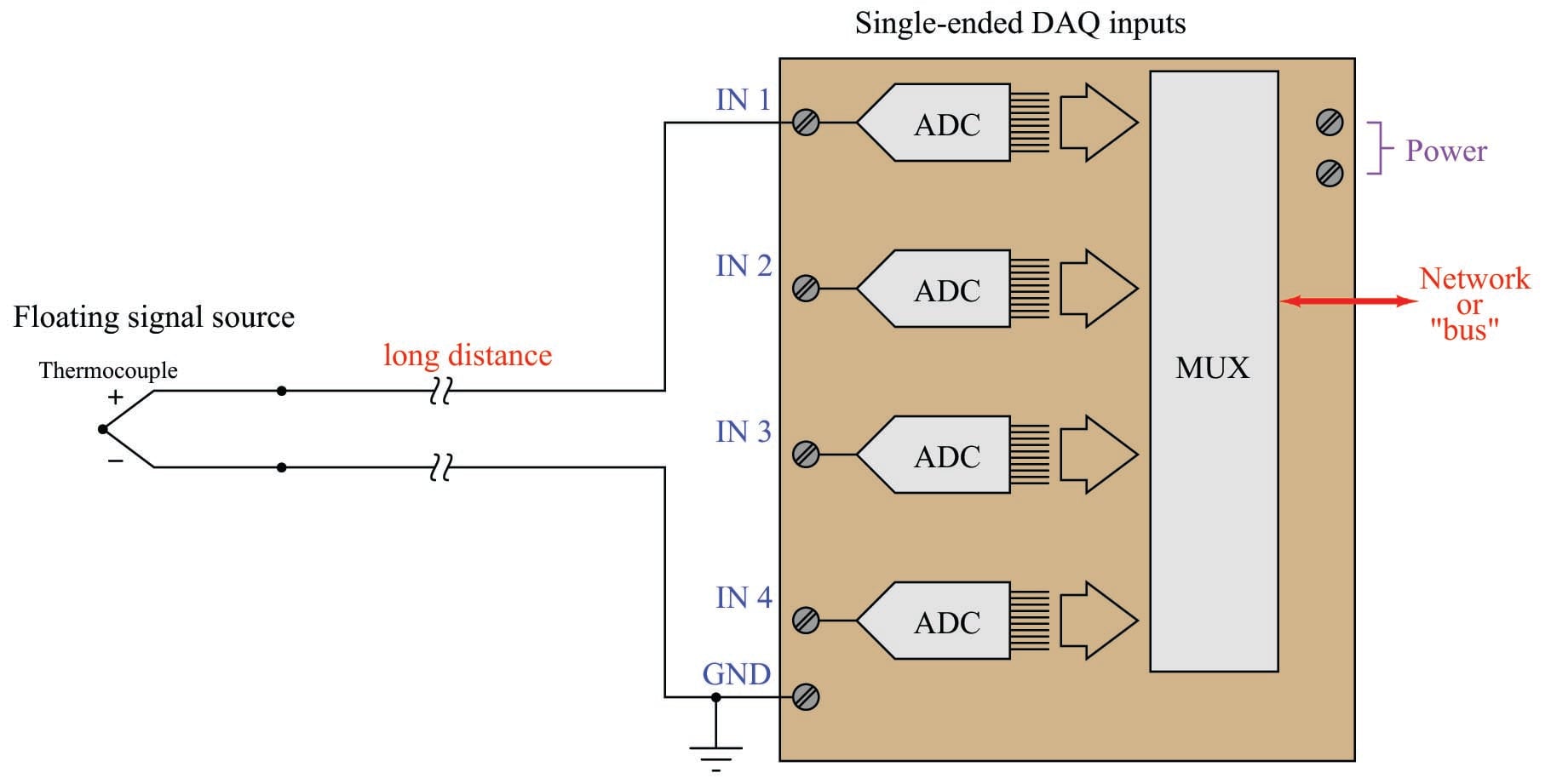
Since an ungrounded thermocouple has no connection whatsoever to any ground, there will be no ground loop when connected to a single-ended DAQ input. The same is true for battery-powered sensor circuits lacking connection to earth ground:
Single-ended analog DAQ inputs have trouble measuring elevated signal voltages regardless of distance. Here, we see an example where someone has tried to connect a single-ended DAQ input to a grounded-excitation RTD bridge, with common-mode voltage equal to one-half the excitation source voltage. The result is disastrous:
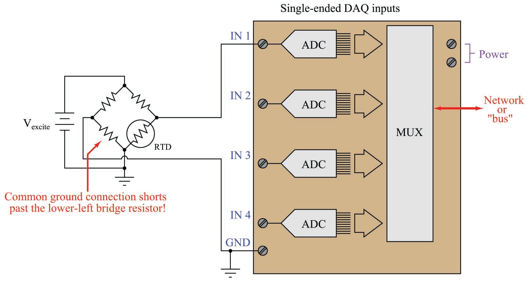
If you follow the bottom wire in this diagram carefully, you will see how it effectively jumpers past the lower-left resistor in conjunction with the two ground connections. Yet, eliminating the wire simply substitutes one problem for another: without the bottom wire in place, the voltage seen by input channel 1 on the DAQ will be \(V_{signal} + V_{common-mode}\) rather than \(V_{signal}\) all by itself.
A clever way to solve the problem of measuring elevated signal sources is to use two analog DAQ channels: one to measure \(V_{signal} + V_{common-mode}\) and the other to measure \(V_{common-mode}\), and then digitally subtract one measurement from the other. Thus, two single-ended input channels may function as one differential input channel.
Here, we see an example of this measurement technique applied to the grounded-excitation RTD bridge:
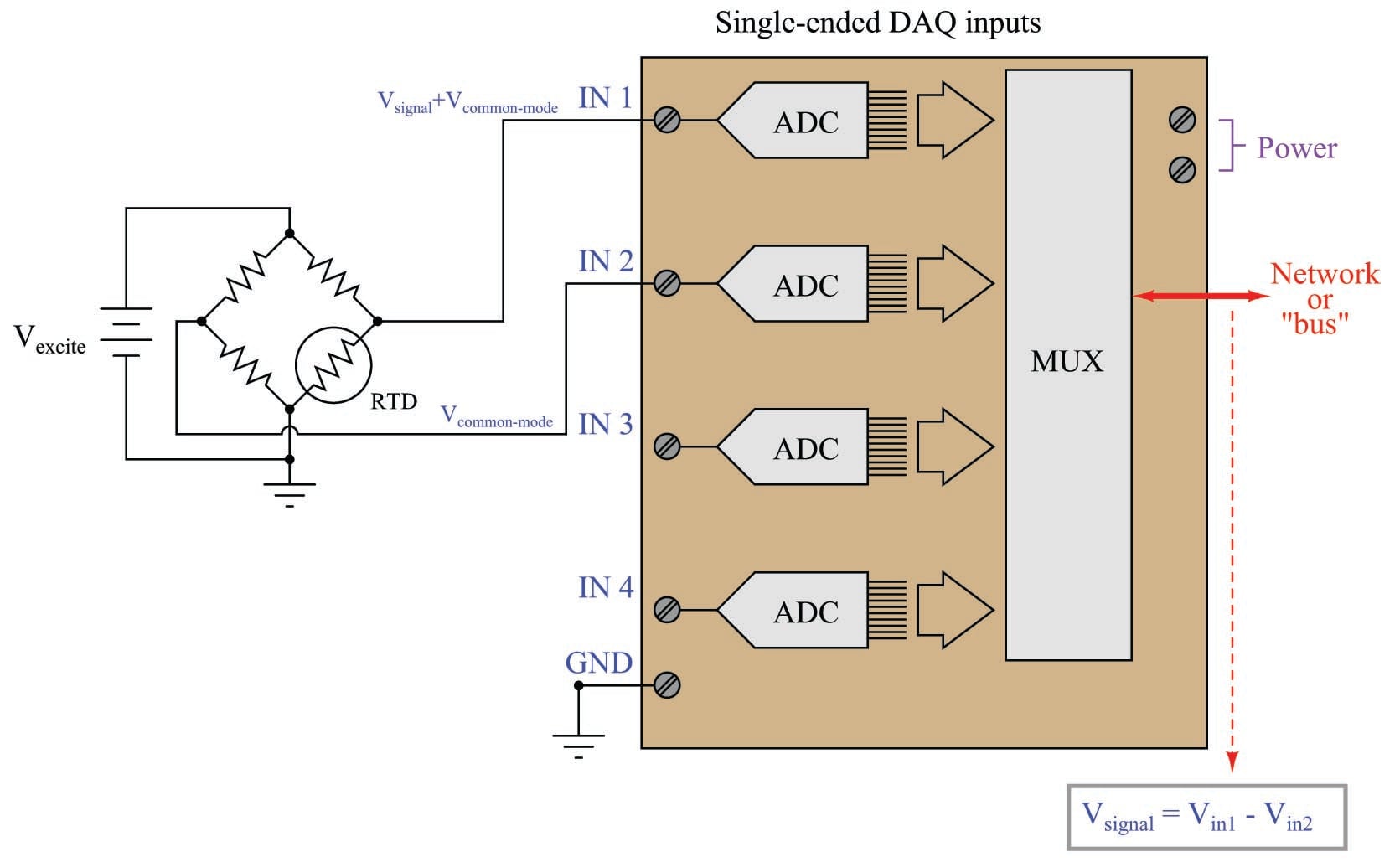
The subtraction of the two channels’ digitized values may take place in a controller separate from the DAQ module, or within the DAQ module if it is equipped with enough “intelligence” to perform the necessary calculations.
An added benefit of using this dual-channel method is that any noise voltage existing between the signal ground and the DAQ ground will be common to both channels, and thus should cancel when the two channels’ signals are mathematically subtracted.
A more versatile hardware solution for measuring any form of voltage signal is a DAQ equipped with true differential input channels. Here, each ADC is equipped with its own instrumentation amplifier, measuring the difference in potential between two ungrounded input terminals:
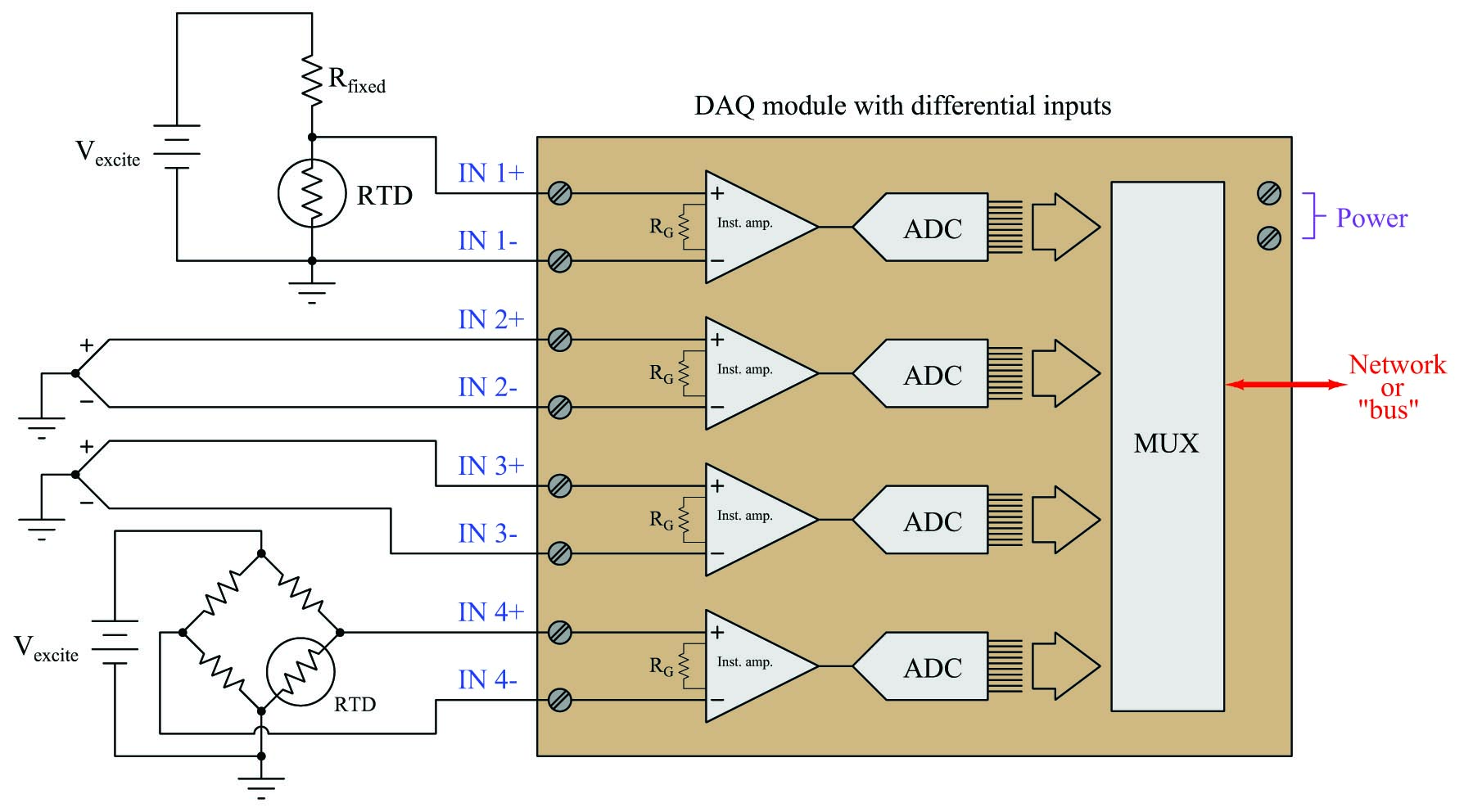
In this example we see one DAQ module measuring four different voltage signal sources, with no interference from differential ground potentials or between the sources themselves. Each input channel of the ADC is electrically independent from the rest. The only limitation to this independence is a certain maximum common-mode voltage between the signal source and the DAQ’s own power supply, determined by the design of the instrumentation amplifiers inside the DAQ module.
One important limitation of differential input channels, however, is that there must be some path for the instrumentation amplifiers’ bias currents to the DAQ’s power supply ground or else the channel will not function properly. This poses a problem where we intend to connect a differential analog input channel to a floating signal source like this:
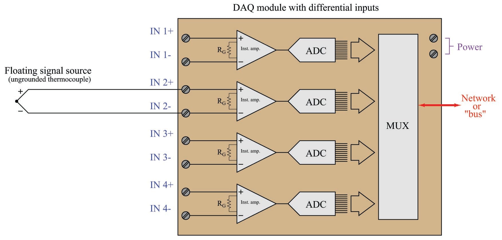
One of the “simplifying assumptions” students learn about operational amplifier circuits is that the input terminals of an opamp draw negligible current. While this may be close enough to the truth when performing calculations on an opamp circuit, it is not absolutely true. All opamps exhibit some amount of bias current at their input terminals, small as these currents may be. Without a complete path to ground for these currents, the input transistor stage of the operational amplifier will not be properly biased, and the amplifier will fail to work as designed.
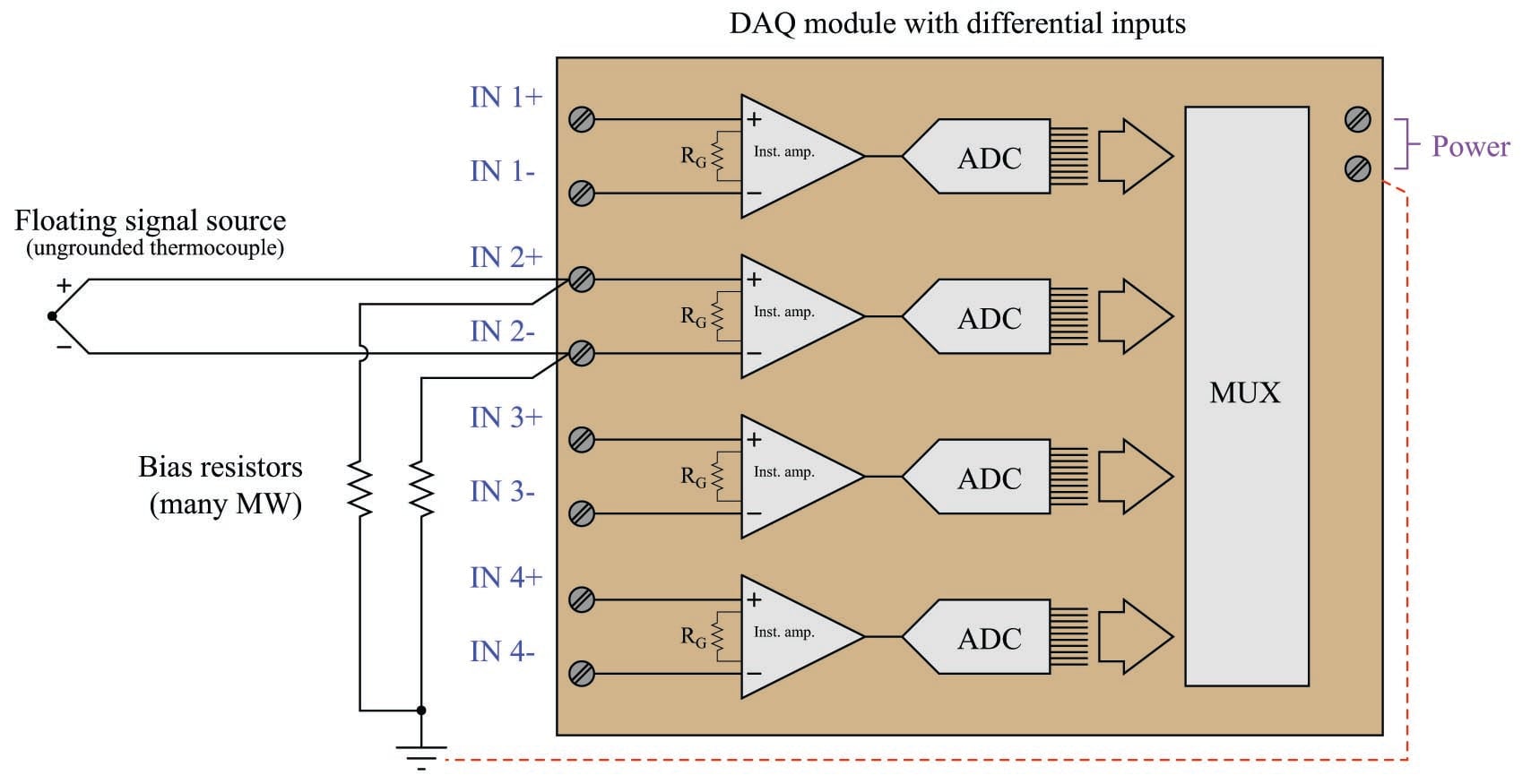
For this reason, we must connect high-value resistors (typically in the mega-ohm range so as not to load the signal voltage being measured) to each of the differential input terminals, and then to ground like this:
In summary, we may list some essential rules to follow when connecting analog DAQ inputs to voltage signal sources:
- Ground points in different locations may not actually be common (enough) to each other
- Never create ground loops through wiring (any conductor connected to ground at each end)
- Beware of common-mode (elevated) signal voltages
- Always ensure a path to power supply ground for amplifier bias currents
