Facebook
 Google
 GitHub
 Linkedin
New Keyence Sensors Target Harsh Detection and Static Control
Designed for tough environments and sensitive wafers, Keyence’s latest sensors focus on durability, fast response, and yield protection.
Detecting metal reliably in harsh environments and controlling static charge in semiconductor fabs remain persistent challenges across manufacturing. A new set of inductive proximity sensors and electrostatic charge sensors addresses both issues with rugged construction and faster detection. Designed for applications ranging from heavy machining to wafer handling, the latest sensor releases focus on improving reliability, protecting equipment, and reducing yield losses caused by environmental exposure and static buildup.
ER Series Inductive Proximity Sensors
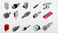
The ER Series is a set of inductive proximity sensors used for determining whether an object is present. These sensors can be used to ensure a workpiece is in place before machining begins to prevent damage to tooling. Typically, it outputs a binary yes/no signal indicating the presence or absence of a metallic object, but some models allow for an intensity measurement. This intensity measurement is a proxy for distance to a metallic object. Some models can detect objects from as far away as 10 mm.
Keyence designed these rugged sensors for heavy machining and tasks in harsh environments. Unlike competing sensors, they feature an all stainless steel body, making them resistant to corrosion, chemicals, water, and other such contaminants. Some models have a ceramic coating that allows them to withstand debris from welding operations. All models are rated to ingress protection IP68G/69K, and are capable of detecting aluminum, copper, or ferrous alloys.
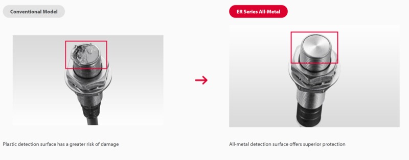
A comparison of plastic-coated sensors versus the stainless steel ER series. Image used courtesy of Keyence
SK Series Electrostatic Charge Sensors
Even a small static charge can arc and damage the wafer irreparably, complete with a microscopic arc flash that can send small particles to damage nearby chips as well. No visible spark is needed to cause significant damage.
The SK Series electrostatic charge sensors can detect as little as 1 V of static charge buildup on objects such as semiconductor wafers. Once detected, the wafer can pass through an ionizer stage to remove the static charge and perhaps save a few of the chips, increasing the overall yield. Furthermore, implementing a pair of these sensors–one before and one after the ionizing step–can ensure that charge dissipation is actually occurring.
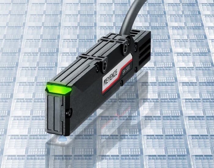
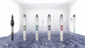
The SK-300 electrostatic charge sensor. Image used courtesy of Keyence
The sensor itself is fast, responding in 28 ms, or 14x faster than conventional sensors, and much faster than hand-scanning. Real-time monitoring is possible through RS232C, EtherCAT, and several other standard industrial protocols, and up to 8 sensors can be connected together for a clear picture of how the process is being affected by static accumulation.
Potential Applications
The ER Series proximity sensors are durable and ruggedized, making them suitable for places that see occasional chemical exposure, water spray, dust, and other environmental contaminants. The stainless steel housing also makes it less prone to damage from occasional abrasion and contact with objects.
Specifically, the SK Series charge sensors will benefit the semiconductor industry. Static buildup on wafers is a major limiting factor, reducing chip yield. The charge sensors can notify operators about charge accumulation and allow them to dissipate that charge before it causes further damage.