Facebook
 Google
 GitHub
 Linkedin
Applied Materials Introduces New Playbook for Process Control Based on Big Data and AI
Applied Materials introduces its three-component solution for chipmakers in its Enlight Optical Wafer Inspection System, ExtractAI technology, and SEMVision eBeam Review System.
Applied Materials Inc. is a leading global provider of materials engineering solutions. The company supplies a range of services, equipment, and software for manufacturing semiconductor integrated circuit (IC) chips. These chips end up in much of the devices used in society today, such as smartphones, homeware appliances, computers, televisions, flat panel displays, and other electronics.
Recently, Applied Materials released a new playbook for process control that brings together Big Data and AI (artificial intelligence) technology for chipmaking technology. The company's solution comprises key components that work together in real-time—identifying and classifying defects during chipmaking. Applied’s solution has been designed to be more cost-effective and time-efficient than legacy approaches.
Challenges of Chipmaking
It is no secret that as the demand for semiconductor chips continues to grow, the cost of fabrication increases. Companies worldwide are looking for innovative ways to produce chips quickly and generate enough yield to improve revenue and profitability. Speeding the time to market can save semiconductor fabricators billions.
The challenges facing chipmaking include increased costs of scanning wafers, which reduces inspection points and specific defects that can cause node delays. Since 2016, Applied Materials has been developing its new playbook for process control, turning the spotlight onto three core components.
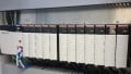
The Enlight Optical Wafer Inspection System
Applied’s Enlight System was designed to be the industry’s fastest high-end optical scanner. Customers can expect a threefold cost improvement in critical defect detection. The system includes brightfield and greyfield optical detection and the highest numerical aperture available.

The Enlight Optical Wafer Inspection System. Image used courtesy of Applied Materials
A multi-patterning approach means more inspection points, and line-health monitoring provides more inspection data for excursion prediction and detection. These combined features allow users to collect more yield-critical data per scan and detect excursions quicker. Wafer processing can be temporarily stopped to protect yields and allow for root-cause traceback. This can aid in more efficient maintenance and faster remobilization of manufacturing.
ExtractAI Technology
Applied Materials combines the Enlight System with ExtractAI to enable defects to be distinguished among noise produced by optical scanners. Quick and accurate detection of yield-killing defects is what Applied aims to achieve here.
The AI system can generate a map of potential unclassified defects and an actionable map of classified defects. This can help semiconductor fabricators enhance development, ramp, and yield.
SEMVision eBeam Review System
Through the SEMVision eBeam Review System, Applied Materials allows users to train the Enlight system with ExtractAI technology to detect yield-killing defects among noise. Learning is active and takes place in real-time using database-to-database connectivity. This provides an adaptive run-time classification of yield-killing defects and noise.

Applied Materials Enlight System, ExtractAI Technology, and SEMVision System. Image used courtesy of Applied Materials
With the Enlight System, EtractAI technology, and SEMVision eBeam Review System working together in real-time, customers can detect new defects as they appear during manufacturing flow. Through this unique solution, Applied Materials aims to increase its customers’ profitability by generating higher yields.