Facebook
 Google
 GitHub
 Linkedin
Counters with OpenPLC: Count Down Instructions on an Arduino Project Kit
Counting is a fundamental task for any process controller. Learn how to implement a PLC counter instruction (CTD) with an Arduino or compatible board using the OpenPLC Ladder Diagram (LD) platform.
Check out the Arduino OpenPLC project articles:
Simplified Prototyping: OpenPLC on an Arduino-Compatible Project Kit
PLC Ladder Logic on an Arduino: Introduction to OpenPLC
PLC Ladder Logic on an Arduino: Building a Start-Stop Circuit
The IEC 61131-3 Functional Programming specification uses a Function Block (FB) for providing a Count Down (CTD) instruction. The CTD FB allows a decrement feature used in a variety of counting event industrial applications like conveyor parts tracking and cascading counter-based flashers. Learn to prototype a basic CTD counter on an Arduino compatible board with an OpenPLC CTD FB.
Count Down (CTD) Function Block (FB)
A CTD FB allows decremented events to be tracked and used as a control mechanism for industrial machine applications. Imagine a conveyor system moving boxes to the packaging stage while tracking the completion of units on a planned total amount. With the total amount entered in a PLC counter tag, the controller will decrement the value based on the completed boxes upon receiving a signal from a proximity sensor. The conveyor will stop running when the cardboard boxes have been assembled and counted. A typical IEC 61131-3 CTD FB is shown in Figure 1.

Figure 1. A Count Down Function Block.
The typical CTD FB pins are labeled and defined as follows.
-
CD (Count Down input) - an external event decrements the counter.
-
LD (Load) - (sometimes called Reset) A control signal to load the Preset value to the FB.
-
PV (Preset Value) - The CTD FB’s counting value. Typically the preset values are positive, non-zero quantities.
-
Q (Output) - The output for the CTD FB, active when CV > PV.
-
CV (Current Value) - The actual current value of the CTD FB.
With the appropriate event-triggered devices and the provided PV and LD values included in the Tag listing, the OpenPLC ladder diagram can easily be built. To illustrate this use of the CTD FB, the following PLC program will be discussed. The example follows the traditional format of an Allen-Bradley (Rockwell) CTD instruction program from an RS500 development interface.
Sample CTD Counter Instruction PLC Program
A typical Allen-Bradley (Rockwell SLC 500) PLC ladder logic program is represented in Figure 2 below. This foundation will be used as a reference ladder logic program to implement as an OpenPLC control application using the CTD FB.
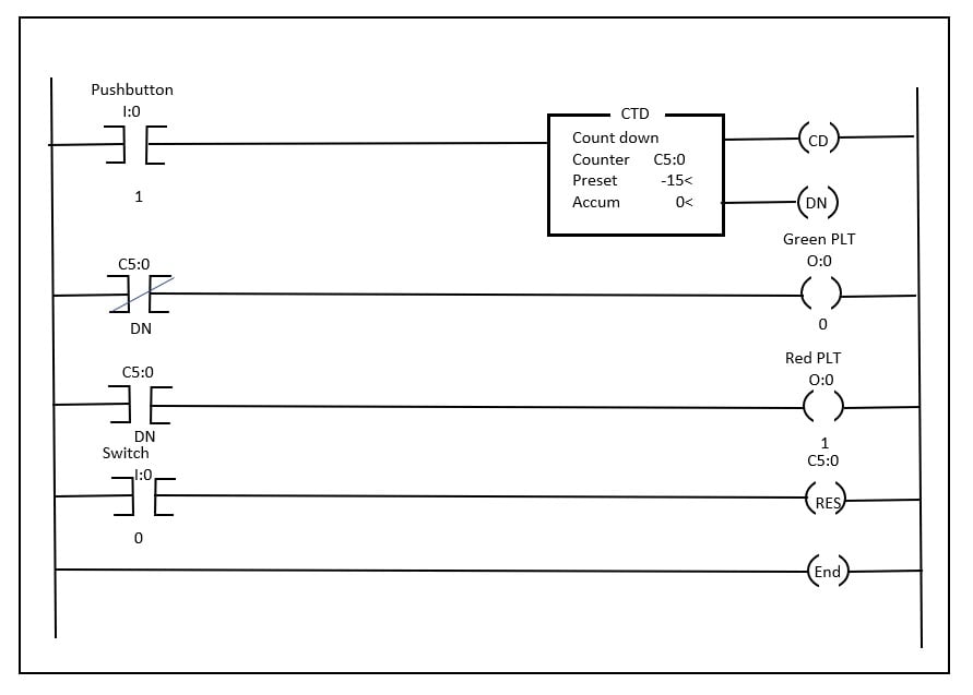
Figure 2. A sample CTD control application PLC ladder logic program as seen in an Allen-Bradley (Rockwell) RS500 interface.
The sequence of events (SoE) for the OpenPLC program implemented on the Arduino compatible control board consists of the following steps.
-
The Green PLT (pilot light) will be ON
-
Press/release the pushbutton switch attached to the CTD Instruction 15 times.
-
When the preset and accumulated values are equal, the Red PLT will turn ON
-
The Green PLT will turn OFF
-
Press/release the Switch will reset the CTD
-
The Red PLT will turn OFF
-
The Green PLT will turn ON
An OpenPLC ladder diagram will be created to perform the CTD control application outlined in the listed SoE. The first step is to create a Tag listing for the OpenPLC CTD counter application.
Freenove Projects Kit Conundrum
In the previous OpenPLC technical article, the Freenove Projects kit board was introduced. The article provided information on the electronic subcircuits of the kit, which allows a convenient method of prototyping ladder logic control applications using OpenPLC. As observed in the previous article, several of the board’s digital input-output (I/O) pins are assigned to populated PCB electronic circuits or components. These digital I/O pin assignments are illustrated in Table 1.
Digital In |
Address |
Application |
Arduino Pin |
|
2 |
%IX0.0 |
KEY1 |
D2 |
|
3 |
%IX0.1 |
KEY2 |
D3 |
|
4 |
%IX0.2 |
KEY3 |
D4 |
|
5 |
%IX0.3 |
KEY4 |
D5 |
|
6 |
%IX0.4 |
Buzzer |
D6 |
Digital Out |
|||
|
7 |
%QX0.0 |
Relay |
D7 |
|
8 |
%QX0.1 |
IR Remote |
D8 |
|
12 |
%QX0.2 |
Stepper Motor |
D12 |
|
13 |
%QX0.3 |
Blue LED |
D13 |
Table 1. Freenove Digital I/O pin assignment table.
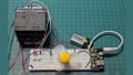
An obvious concern is that with the digital I/O pins and their assigned addresses, the Freenove Projects Kit board may not be able to expand to external electronic circuits. With such rigid wiring to the populated electronic circuits provided by the Freenove Projects Kit board, external device prototyping OpenPLC ladder diagram concepts are impossible. The solution to this possible conundrum is the DIP switches. The soldered DIP switches provide a convenient approach to connecting or disconnecting from the populated electronics by simply opening or closing the pre-mounted circuits, as shown in Figure 3.

Figure 3. Electrically connecting to the Transistor-Relay circuit (D7) with a DIP Switch.
As illustrated in Figure 3 and documented in Table 1, the Freenove Control board digital pin D7 is assigned to the transistor relay circuit. To operate and connect with the electronic circuit means to close the switch. The closed switch will be in the ON position, thereby electrically connected to digital pin D7 of the Freenove control board.
The remaining switches for inputs and outputs will be placed in the appropriate positions as shown below in Figure 4, referenced from Table 1 above.
-
Pin D2 on the control board is address IX0.0, attached to Switch 1.
-
Pin D3 on the control board is address IX0.1, attached to Switch 2.
-
Pin D7 on the control board is address QX0.0, attached to the Relay.
-
Pin D13 on the control board is address QX0.3, attached to the Blue LED.
With the kit powered up using a USB cable, the LED indicators D2 and D3 will be illuminated. Pressing either the S1 or S2 pushbutton switch will turn OFF the I/O LED indicators. To ensure the transistor relay circuit, the Blue LED, and digital inverted logic switches are electrically connected to the appropriate Freenove Control board digital pins, slide the corresponding DIP switches to the ON position. Figure 4 illustrates the DIP switches.

Figure 4. Appropriate DIP switches are placed in the ON position.
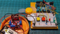
The complete electronic circuit schematic diagram of the I/O devices to be electrically wired to the Freenove Control Board is shown in Figure 5. With the appropriate DIP switches placed in the ON position, these electronic subcircuits will be operational once the OpenPLC ladder diagram program is uploaded to the control board. Opening the DIP switches will prevent the correct operation of the OpenPLC ladder diagram program from occurring. The next step in the OpenPLC control application project is building the ladder diagram program

Figure 5. The CTD counter electronic circuit schematic diagram.
Equivalent Breadboard Circuit
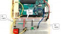
For those who do not have the Freenove Project Kit, this circuit can easily be constructed with two switches and two outputs. For this example, to maintain consistency, the same pin address connections will be used as in Figure 5.

Figure 6. Breadboard equivalent, with input switches connected to D2 and D3, output LEDs connected to D7 and D13.
OpenPLC CTD Counter Control Circuit
The Tag listing for the OpenPLC CTD counter control application is shown in Figure 7. The tag listing provides the digital I/O addresses for the external switches and output control devices wired to the Freenove Control board. Notice that the Load value and the Preset value have a 5 as the initial number. This low numeric value will demonstrate the CTD FB’s counting function quickly.

Figure 7. CTD counter application tag listing.
OpenPLC CTD Counter Ladder Diagram Program
The OpenPLC CTD ladder diagram shown in Figure 8 below is the IEC 61131-3 equivalent program to Figure 2.
To include the CTD FB, select the FB icon within the OpenPLC top taskbar. Select a location on the OpenPLC ladder diagram editor. The function block window will appear; select the CTD FB from the various listing of counters.
The use of normally closed (NC) contacts in the diagram below is due to the fact that the Freenove inputs are normally closed themselves. If you are building this project using breadboard switches, normally open (NO) switches would be the correct choice to use.

Figure 8. OpenPLC CTD counter control ladder diagram application
Figure 9 illustrates the steps to obtaining the CTD FB within the OpenPLC taskbar.

Figure 9. The placement of the CTD FB.
With the CTD FB placed on the OpenPLC ladder diagram editor, upload the software to the Freenove Control board. Now you can test the operation of the control application using the SoE provided on the ladder diagram shown in Figure 8. Here is a video clip illustrating the steps and the operation of the count down counter control application.
Next time, exploring up counters using the Count Up (CTU) FB will be presented.
Interactive Quiz: FPK Start-Stop Control LD Program Solution
Use address %QX0.3 to operate the Blue LED with the Start-Stop Control LD program.
Technical Quiz: Solution
Switches S1 and S2 are digital inverted logic switches. To ensure a binary logic 1 (+5V) is presented when pressing the switches, the inverted or negated bit instructions will provide properly aligned control signals for the correct Start-Stop logic operation.